LIBRARY
Monolithic Optoelectronic Integration of GaN High-Voltage Power FETs and LEDs with a Selective Epi Removal Process
Monolithic optoelectronic integration increases the maximum modulation frequency by lowering the parasitic inductance at least two orders of magnitude when compared to a discrete packaged LED and power FET. We employ a lateral, enhancement-mode MOS-Channel-HEMT (MOSC-HEMT) [1] as the power transistor in combination with a quasi-vertical LED all on one substrate.
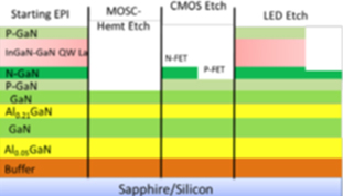
The Selective epi Removal (SER) approach employs the growth of the epi for the LED on top of the epi layers for electronic devices, as shown in Figure 1. Then it selectively etches the epi layers away to process the GaN electronics, allowing devices to share common epi layers and thus, saving processing costs. SER also eliminates the need to implement any epi re-growth steps, saving fabrication time. SER enables the emitted light to be extracted from either the top or the bottom of the LEPIC. The first full integration of a GaN LED and MOSC-HEMT is underway; however, the process has been validated with a short loop MOS capacitor lot. The two largest technical barriers with this approach are: 1) not compromising the quality of the electronic epi during the LED epi growth and 2) removing all of the LED epi in the areas where FETs are to be fabricated, without over-etching. The short loop MOS capacitor experiment was designed to verify that both of these barriers can be overcome.
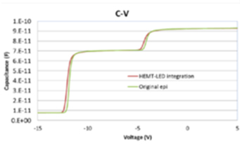
To confirm the growth of the LED epi did not substantially affect the electronic epi, the 2DEG concentration was measured using a MOS capacitor on two samples, one without LED epi growth, and one with LED epi growth. After the LED epi was grown, half the sample was masked off, and the other half was etched down to expose the electronic epi. In this area, MOS capacitors were fabricated. If the bottom layer of the LED was not removed, the MOS capacitor would not be able to be depleted. If the thin electron generating layer was removed by an over etch, the MOS capacitor would be depleted too easily. The 2DEG concentration of the sample without LED epi was 3.2e12/cm2 while the sample with LED epi was 3.0e12/cm2, see Figure 3 and 4. These results confirm that the LED growth cycle was not detrimental to the electronic epi, and that the etch depth can be controlled well enough to isolate the MOSC-HEMT epi from the LED epi. We are in the process of making prototype circuit building blocks which integrates high-voltage MOSC-HEMTs and LEDs.
