LIBRARY
High-Temperature Characterization and Comparison of 1.2 kV SiC Power Semi-conductor Devices

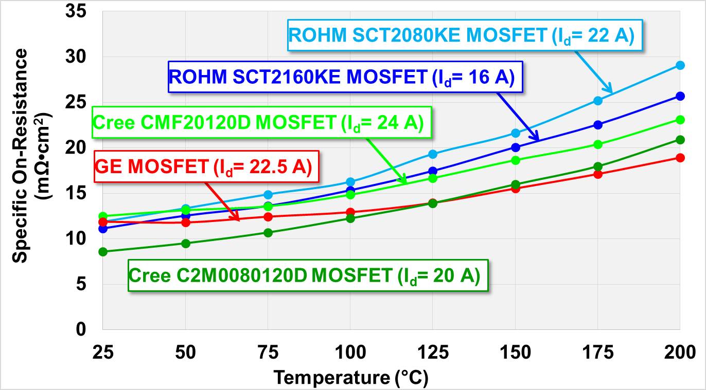
Fig. 1 shows the measured specific on-resistance versus temperature. The drain current used for the measurements is shown in parenthesis for each curve. The gate-source voltage used for the on-resistance measurement was 20 V since this is the voltage at which the MOSFETs will be driven. As seen in the figure, the GE MOSFET is the least temperature dependent, increasing by approximately 37% at 200C with respect to its room-temperature resistance.
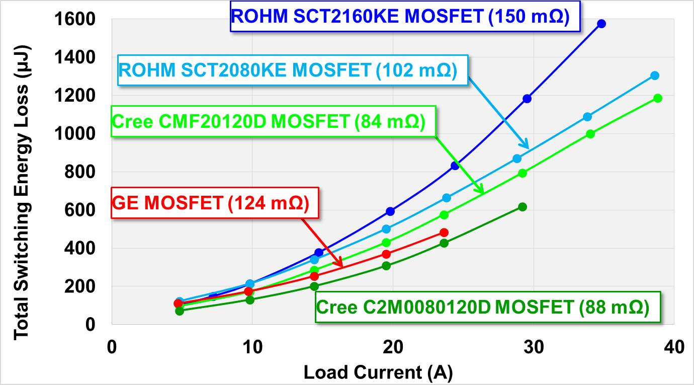
DPTs were performed on each SiC MOSFET with a DPT setup specifically designed to reduce the parasitic components that inhibit switching performance. The optimal driving condition for each SiC MOSFET was determined by performing multiple DPTs for several different external gate resistances RG, ext to account for the variation in internal gate resistance described above. The external gate resistance that yielded the lowest switching energy loss without causing significant ringing was selected. Due to the large internal gate resistance of the ROHM SCT2160KE MOSFET, even when no external gate resistance is used the total gate resistance is still nearly double that of the other devices. Consequently, although the ROHM SCT2160KE MOSFET proved to have low junction capacitances, the device can be expected to experience higher losses. Fig. 2 shows the total switching energy loss plotted against load current. DPTs revealed that the majority of the switching losses are experienced during turn on, thus soft switching could be applied in order to increase switching efficiency.


