


LIBRARY
A Novel Hybrid Packaging Structure for High-Temperature SiC Power
Year: 2014
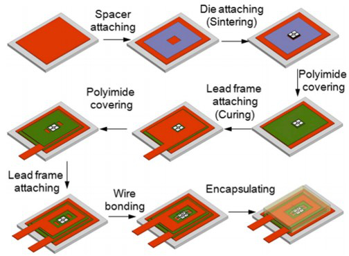
Fig. 1. Hybrid-structure packaging fabrication process.
Fig. 1 shows the fabrication process with a single SiC JFET. The processing time is two hours less than that of the planar structure. In addition, the planar packaging structure employs a three-step sintering process, and each process temperature be at least 40°C lower than the previous one to prevent it from melting. This makes it difficult to select the die-attachment materials. However, since there is only one sintering process in the hybrid packaging structure, more flexible die-attach material selection is possible. The fabricated power module is shown in Fig. 2. There are three input power lead frames (A, B, and C), two output power lead frames (P and N), and two gate-drive lead frames (G and S). The lead frames are fabricated separately with a DBC substrate.
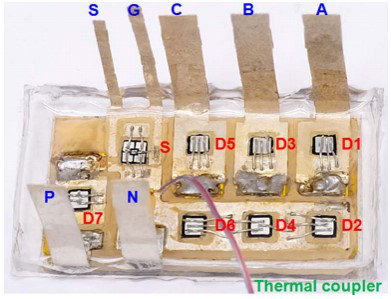
Fig. 2. Multiple-chip power module.
