LIBRARY
Characteristics of Monolithically Integrated LED/Power MOS Channel HEMT Pair in GaN with Selective Epi Removal

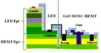
The GaN LED and GaN MOSC-HEMT are monolithically integrated using the selective epi removal (SER) process approach. The starting HEMT epi is on a sapphire substrate, and an LED epi is grown in-house on top. The integrated LED and MOSC-HEMT structure is fabricated by first removing selected regions of the LED structure to expose the HEMT epi using ICP-RIE. Subsequent fabrication processes of the LED and MOSC-HEMT are carried out with multiple shared steps. Finally the interconnection metal connects the LED cathode to the MOSC-HEMT drain, forming a series configuration, as shown in Fig. 1.
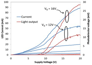
Detailed electrical and optical characteristics of the integrated GaN LED/HEMT pair are measured at 25 °C and up to 225 °C. The GaN LED emits a bright blue light, which is directly driven by the integrated MOSC-HEMT. The room-temperature (25 °C) LED current and light output intensity are measured as a function of the supply voltage and the HEMT gate voltage, showing that the light output has been successfully modulated by the gate voltage of the MOSC-HEMT with good linearity (Fig. 2). With the temperature rising, the light output power at the same driving current of the LED/HEMT pair shows an obvious decrease. The results demonstrate the compatibility of III-nitride LED and HEMT processes. The high-temperature performance of the integrated GaN LED is comparable to that of discrete GaN LEDs. The integrated GaN LED emission spectrum is dependent on current and temperature. A dominant wavelength of 459 nm has been extracted, with a FWHM as small as 22 nm.


