


LIBRARY
4H-SiC P-i-N Diodes on Lightly Doped Free-Standing Substrates
Year: 2015
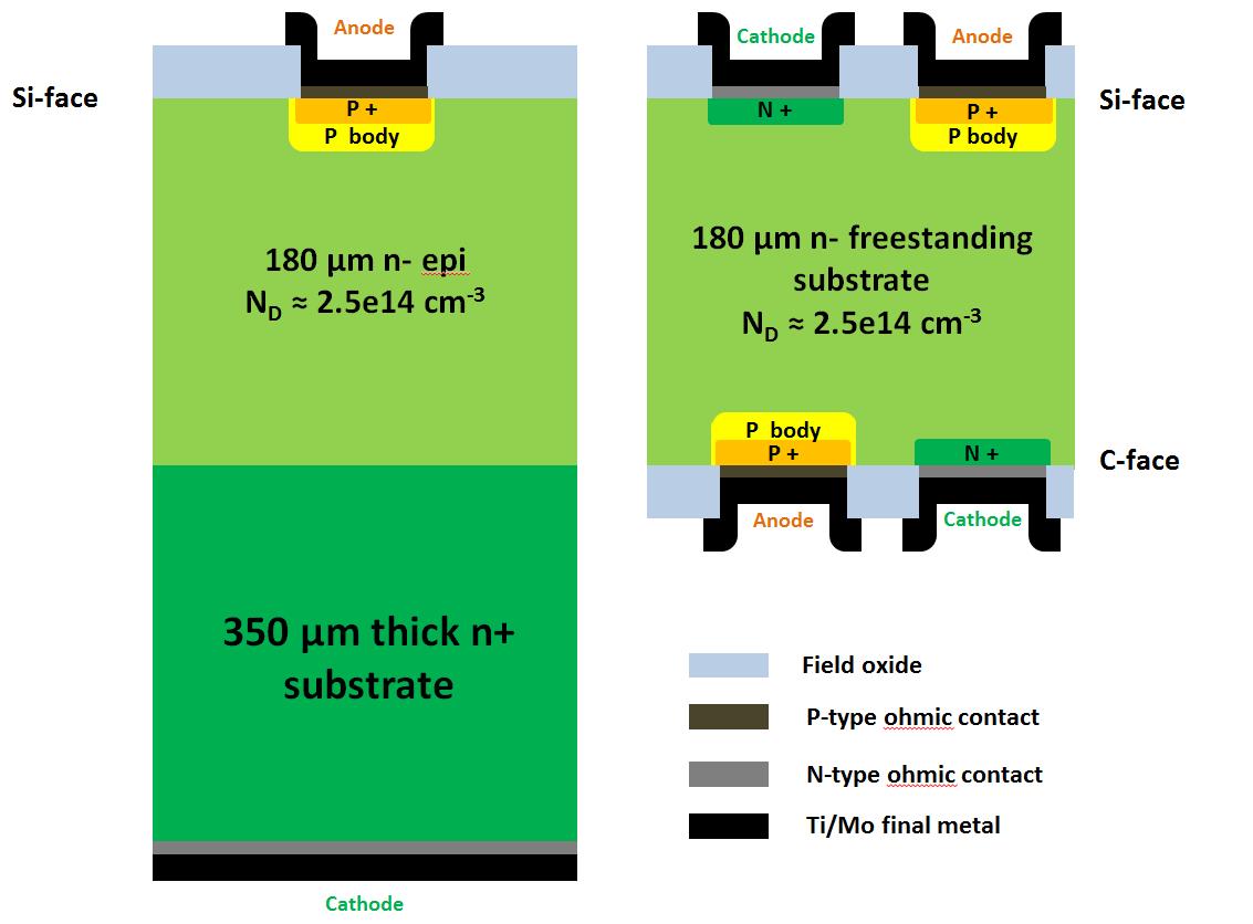
Fig. 1 Schematic cross-section of fabricated diodes
4H-SiC samples with a thick, lightly doped epi layer (WD = 180 µm, ND = 2.5e14 cm-3) on a 4o off-axis n substrate were obtained from a commercial vendor. The FSS samples were obtained by selective removal of the n substrate. The high level carrier lifetime of 1.5 - 2.5 µs was measured by microwave photoconductive decay (MPCD). Fig. 1 shows a cross section of the fabricated devices. Microwave photoconductivity decay (MPCD) measurement before and after the n substrate removal indicates no degradation of carrier lifetime during the substrate removal process. This is also confirmed from the electrical characterization of the fabricated pin diodes.
Fig. 2 shows the forward I-V of the various diodes at 200 oC. The extracted device parameters are summarized in Table 1. Higher VF and ron in FSS diodes can be expected because of the ad-ditional defects created under the cathode region during the high dose phosphorus implant. The ideality factor (n) for Si-face diodes (both conventional and FSS) shows a minimum value of 1.33. This is in agreement with the multiple trap level recombination model with 1 deep level and 2 shallow levels. The current in C-face FSS diodes shows a power law relationship at low currents (J ~ V6). This is indicative of space charge limited current and has been previously observed in 6H-SiC pin diodes. Both conventional and FSS diodes show a low leakage current (Jleak ≈ 0.2 µA/cm2 at VR = 100 V). Both conventional and FSS diodes show a lifetime between 2.5 - 3.0 µs at 25 oC, which increases to about 4.5 µs at 200 oC. These values agree well with lifetime measured by MPCD method prior to device fabrication. All the diodes show a similar reverse recovery characteristics with QRR = 7.5 µC/cm2 and tRR = 90 ns and JRP = 200 A/cm2 at room temperature.
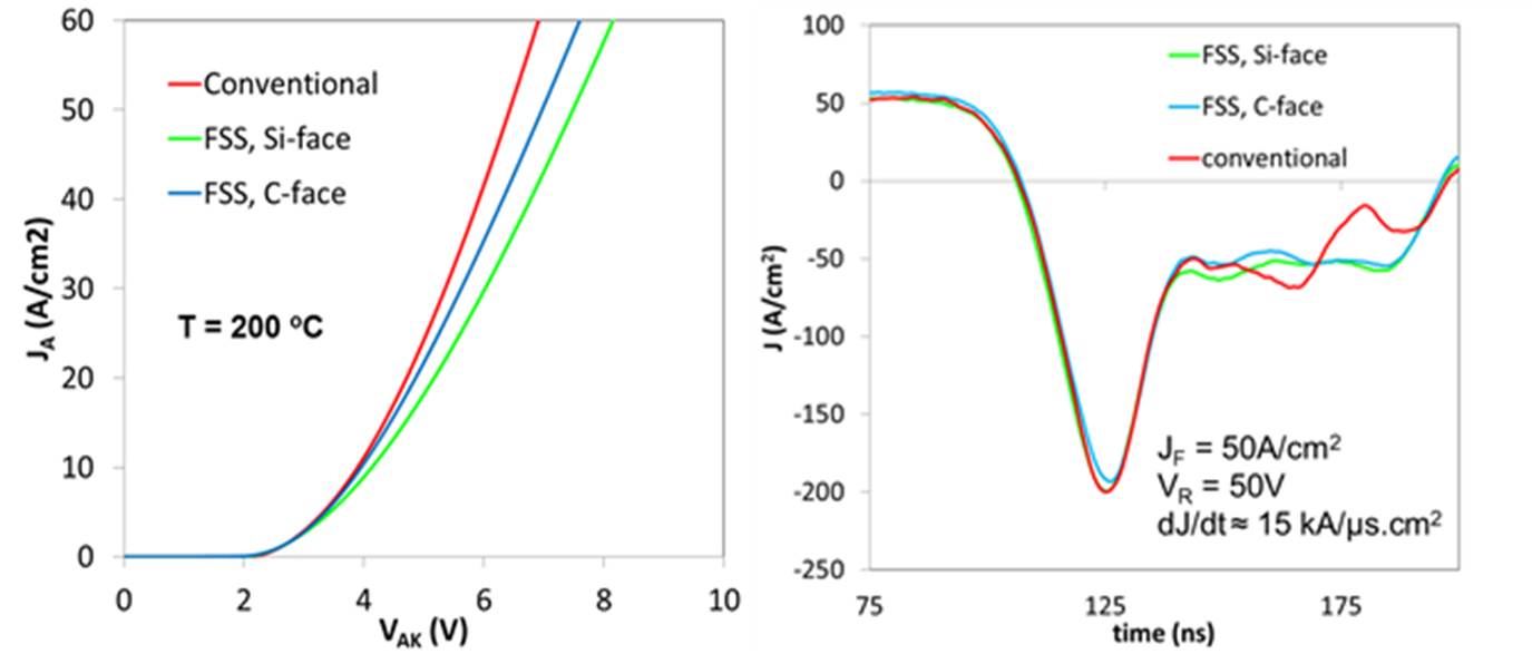
Fig. 2 Forward I-V and reverse recovery characteristics of the fabricated pin diodes

