


LIBRARY
Temperature Cycling Reliability Assessment of Die-Attachment on Bare Copper by Pressureless Nanosilver Sintering
Year: 2015
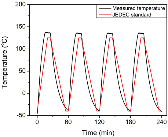
Fig. 1. Measured temperature cycling profile in comparison with JEDEC standard
Nanosilver paste, an emerging die-attach material, was formulated by mixing nanosilver particles with several types of organic additives. Extensive research has been done on the ap-plication of nanosilver paste for die-attachment. It has been demonstrated that nanosilver paste can be applied for attaching power devices of different sizes onto silver and gold surfaces by pressureless or low-pressure-assisted (< 5 MPa) sintering, with sintering temperature lower than 280 °C.
The goal of this study was to evaluate the temperature cycling reliability of the pressureless, forming-gas-enhanced sintering process for bonding chips on copper using nanosilver paste. Thick silicon chips were attached to the DBC with a bare copper surface for die-shear testing, while thin silicon chips were attached to copper lead frames for microstructure analysis. Sam-ples were subjected to temperature cycles in the range of -40 °C to 125 °C with a cycling period of 60 minutes. Die-shear tests were performed on cycled samples. X-ray tomography was ap-plied to detect the defects in the die-attach joints for the silicon samples. Microstructures of cross sections of the joints were characterized by SEM.
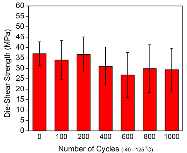
Fig. 2. Die-shear strength of joints versus number of temperature cycles
