LIBRARY
Large Substrates Bonded by Silver Sintering and Their Thermal Performance

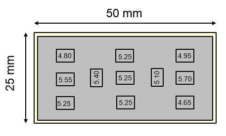
Silicon IGBT chips are mounted on the substrate. The IGBTs are used as a heat source as well as a temperature sensor. Transient thermal impedance or Zth measurement is performed by taking the ratio of junction temperature raise over the heating power. The package is modeled by a Foster network of capacitors and resistors, which corresponds to heat capacities and resistances of the materials or interfaces, respectively. Then, using electrical network theories and mathematical algorithms, the measured junction temperature response is transformed into a cumulative structure function of the package. The function represents a relationship between the cumulative thermal capacitance and cumulative thermal resistance from the device junction through the package. Finally the thermal resistance of the substrate attach layer is derived. By mounting multiple chips at different locations, the 2-dimension map of thermal resistance is plotted as shown in Fig. 2. The average value is 5.20, which is nearly the lowest amongst the thermal interface materials. The variation is 6%, which illustrates the bonding quality is uniform across the whole area.


