LIBRARY
Design and Development of a Novel, High-Density, High-Speed 10 kV SiC MOSFET Module

At present the performance of these unique devices is limited by standard module packages that were originally developed for slower, lower density Si devices. This work aims to fabricate an optimal package for 10 kV SiC MOSFETs that would have minimal parasitic elements to allow for good transient performance, low thermal impedance to effectively remove the heat from the devices, and a small footprint to achieve high power density. The 10 kV rating of these MOSFETs means that high electric fields will be present within the module. Accordingly, care must also be taken to design a layout that will reduce the concentration of these electric fields.
To achieve higher density, and reduce parasitics, the antiparallel diode is eliminated. Instead, the superior reverse conduction characteristics of the SiC MOSFETs are utilized. To minimize the parasitics, molybdenum posts and direct bonded aluminum (DBA) substrates are used for the module connections (forming a planar structure), in place of wirebonds. Embedded capacitors further improve the transient performance of the devices. Finally, to minimize the peak electric field that occurs at the triple point of the DBA substrates, two DBAs are stacked together. The designed power module, which has gate- and power-loop inductances of just 3 nH, is shown in Fig. 1.
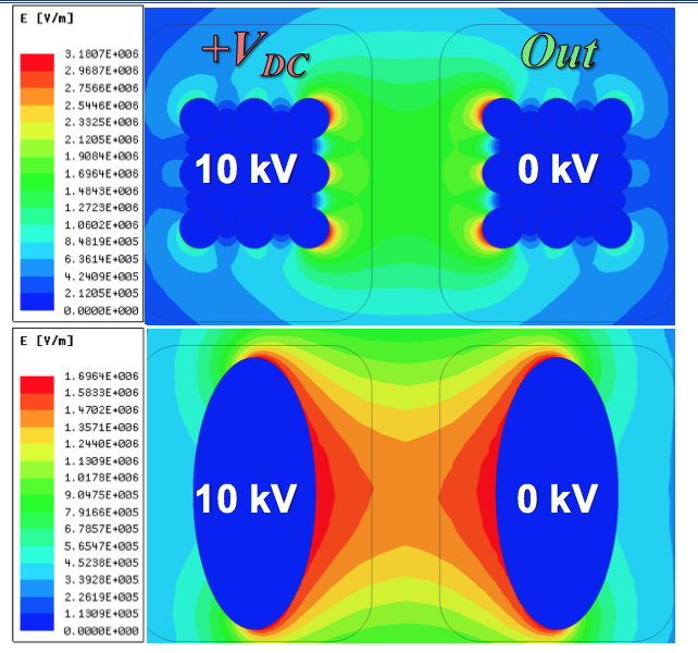
A proper package will also consider the system integration. For instance, when designing the power module, the interface to the gate driver and dc bus bar must be considered. Fig. 2. shows a 2D electrostatic simulation of two different types of power terminations. Due to the high density of the power module, when using pins with small diameters, the electric field concentration exceeds the dielectric strength of air (3 MV/m). By placing conductive elliptical shields around the pins, the electric field can be more uniformly distributed. In this example, the electric field is reduced by nearly half. This results in a higher partial discharge inception voltage.


