LIBRARY
Design of a Novel, High-Density, High-Speed 10 kV SiC MOSFET Module
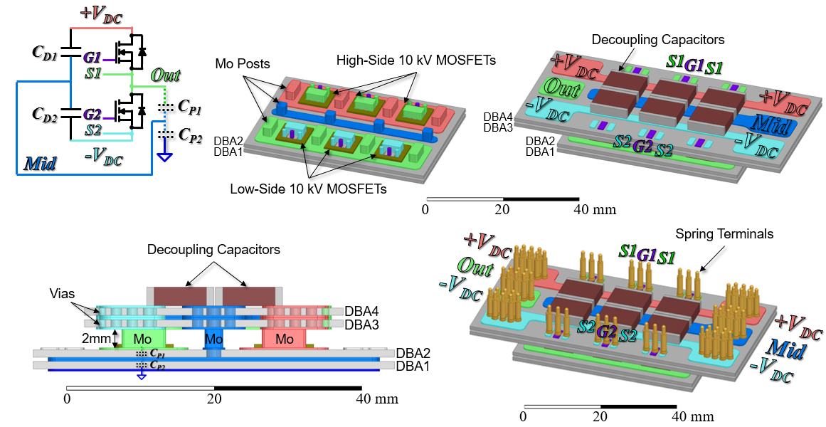
Fig. 1 shows the designed half-bridge module, which has three 10 kV, 350 m&Omega die in parallel per switch position for a total module current of 54 A. The module has a planar structure, using molybdenum (Mo) posts and direct-bonded aluminum (DBA) substrates as the die interconnection instead of wirebonds. This type of structure allows for a higher power density, reduces the parasitic inductances and capacitances in the module, and increases the energy absorption capability (e.g. during faults). This structure also allows decoupling capacitors to be embedded within the module to further improve the dynamic performance. Furthermore, the embedded capacitors and stacked DBA structure can be used to form an integrated screen that diverts some of the generated common-mode current back to the dc bus (Fig. 1). The total module footprint is 35.2 mm × 74.3 mm × 11.4 mm without the housing, giving a power density of 18.1 W/mm3. For reference, the power density of Wolfspeeds 10 kV, 240 A SiC MOSFET module is 4.2 W/mm3, including the housing.
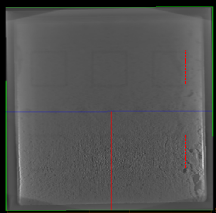
According to ANSYS Q3D Extractor, the gate-loop inductance for each MOSFET die is 3.8 nH. For the power loop, the total parasitic inductance is 4.4 nH with the embedded decoupling capacitors. In order to address the enhanced electric fields associated with a high-voltage, high-density package, two DBAs are stacked on top of each other. By stacking two DBAs, the electric fields both within the ceramic and at the critical triple points, which, in this case, are where the ceramic, metal, and encapsulation meet, are drastically reduced. A pressure-assisted silver-sintering process was developed for bonding the 50 mm × 50 mm substrates. Due to the need for a low thermal resistance of the bonding layer under the die, X-ray scans were performed on the sample (Fig. 2). From these images, no large voids could be observed in the regions where the die will be placed (indicated by the dashed red boxes). Pressureless silver sintering is used for the die and Mo post attach. Solder paste is used to connect the Mo posts to the top DBA substrate in order to provide some compliance and offset any height non-uniformity of the structure.
