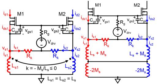
Fig. 1. (a) Passive topology employing negatively-coupled power-source inductors (Ls1/2) and drive-source resistors (Rk) to balance peak currents; (b) equivalent circuit.
The peak currents between two paralleled silicon-carbide (SiC) metal-oxide semiconductor field-effect transistors (MOSFETs) can differ significantly due to a mismatch in threshold voltages (
Vth). The method described in this paper employs passive compensation (drive source resistors and coupled power source inductors) to balance the peak currents using one gate driver, no sensors, and no feedbackwithout increasing total switching losswhen equivalent gate drive resistance (
Rg + 0.5
Rk) is kept constant. This solution works for both polarities of the
Vth mismatch, and forces balancing from the first current peak. The extra voltage stress from this solution is mitigated by negative coupling. The passive components (resistance, self-inductance, and mutual inductance) are determined by an equation involving the magnitude of the
Vth mismatch, current rise time, and the unbalance percentage. The influence of other parasitic inductances on current sharing is analyzed. The robustness of this passive balancing method is experimentally verified by a prototype with a significant amount of parasitic inductances. Test results show that the difference of peak currents can be reduced from 15 to 3 percent without changing the switching loss and voltage stress.
The passive balancing topology with drive source resistors (
Rk) and inversely or negatively coupled power source inductors (
Ls1 and
Ls2) is shown in Fig. 1 (a). The coupled inductors are replaced by the self-inductance
Ls and the mutual inductance
-Ms (Ms > 0) in Fig. 1(b). A realization of negatively coupled inductors is using air core. The waveforms for the baseline design are shown in Fig. 2 (a). Fig. 2 (a) also shows the experimental results of current balancing solution with designed Ls, Rk, and s.

Fig. 2. Experimental switching transients (a) with baseline design, and (b) with the designed Ls, Ms, and Rk. Test conditions were Vin = 300 V, Iin = 20 A, Rg+ 0.5Rk = 20 ?, Vth1 = 2.34 V, and Vth2 = 2.78 V.


