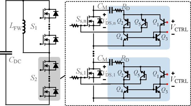
Fig.1. Active dv/dt controller for stacked SiC MOSFETs.
Silicon carbide (SiC) MOSFET devices are gradually supplanting Silicon (Si) insulated gate bipolar transistors (IGBTs). This is due to their ability to operate at higher switching frequencies and higher voltages, and with higher thermal conductivity. Due to these advantages, it is worthwhile to study the use of SiC MOSFETs in the design of higher-power systems. By stacking SiC MOSFETs in series, converters can achieve even higher blocking voltages. Additionally, two-level switching topologies are of interest due to less complex circuitry, higher density, and simpler control techniques, when compared to conventional multilevel topologies, which typically require additional flying capacitors or isolated voltage sources. The main challenge of stacking devices in series is unbalanced voltages across devices, which can be caused by tolerance in device parameters, package and layout parasitic components, and gate signal timing delays. To compensate unbalanced voltages across stacked switches, active dv/dt control can be used with feedback control of each devices drain-to-source voltage (V
DS), as shown in Fig. 1. Compared to other voltage balancing methods, active dv/dt control is preferable, due to its small footprint and low losses. In Fig. 1, Q
1 through Q
4 constitute a bipolar junction transistor (BJT) current mirror network that controls the direction of the current generated by the external Miller capacitor C
M. The capacitor C
M induces a current at the drain of each device, based on the dv/dt at each drain. This induced current is distributed through the BJT network in Fig. 1. The magnitude of the voltage signal V
ctrl determines the magnitude of the Miller current directed to the device gate and the speed of the device at turn-off. The BJT device Q
5 acts as a freewheeling loop for the induced current to circulate and discharge C
M during each turn-on transition. In this paper, the development of a stacked switch with active dv/dt control is detailed. Experimental results for closed-loop voltage balancing of four stacked SiC MOSFETs are evaluated, as shown in Fig. 2. Finally, scalability considerations when stacking more devices in series are discussed.
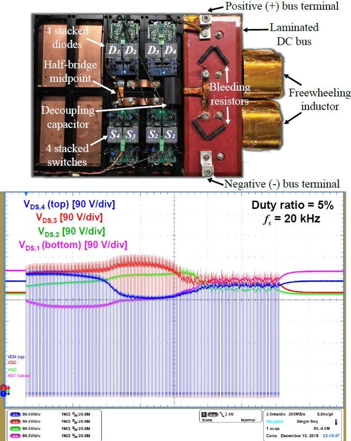
Fig. 2. Closed-loop dv/dt control of 4 stacked SiC MOSFETs with a 2 kV dc bus in a half-bridge configuration.


