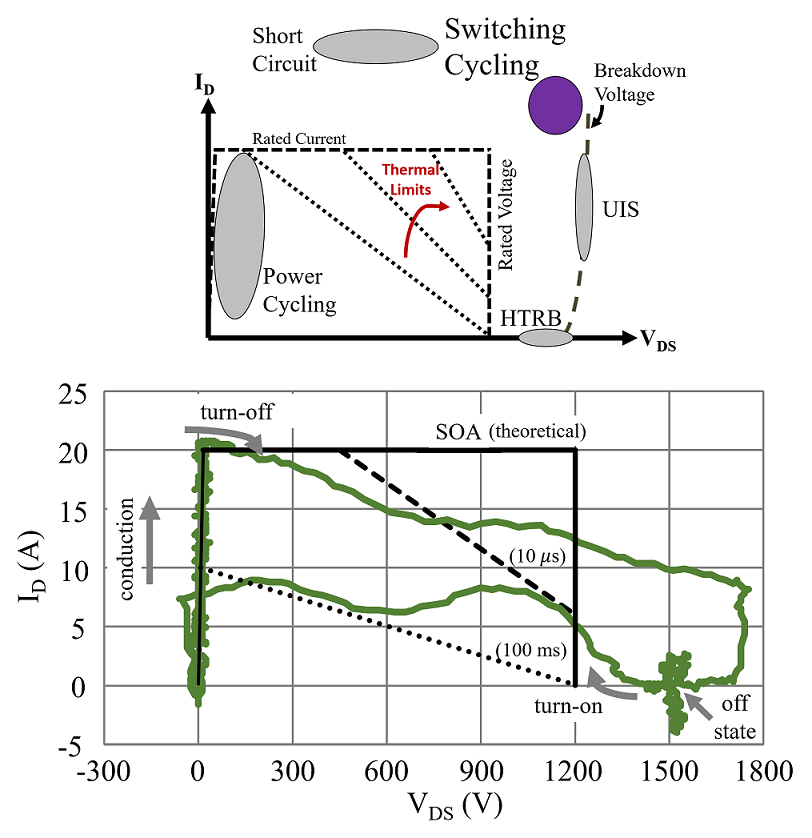
Fig. 1. ALT electrical stress conditions with relation to the SOA (top) and experimental switching cycling IV locus (bottom).
Integrating SiC power MOSFETs is very attractive for advancing power electronic systems, yet system reliability with new devices remains in question. This work presents a newer accelerated lifetime test (ALT) that further investigates the packaging and semiconductor failures of a TO‐247 SiC MOSFET. This ALT, entitled "switching cycling," utilizes the transient turn‐on and turn‐off of a device to stress the semiconductor under high drain‐source voltage (VDS) and high-pulsed drain-source current (IDS). The device is pulsed on to allow it to fully turn on and reach the desired stress current. The short pulse time minimizes conduction losses, therefore mini- mizing self-heating effects. The general stress conditions of different ALT experiments, as well as the switching locus waveform for switching cycling, are shown in Fig. 1.
The objective of switching cycling is to observe the degradation of the semiconductor through repetitive hard switching events. Two independent degradation and failure mechanisms have been identified. While the gate-oxide degradation emerges with the increased switching cycles, bulk-semiconductor degradation appears simultaneously and drives the device into a partially failed‐yet functional‐state before failure. Changes in electrical parameters over time, including threshold voltage on-resistance, gate-leakage, and drain leakage currents are all monitored, and precursors for two degrada- tion mechanisms have been identified. Fig. 2(a) shows the changes in drain leakage for device D
4, and Fig. 2(b) depicts the gate leakage currents over time for all devices.

Fig. 2. Changes in (a) drain leakage current of device D4 and (b) changes in gate leakage current of all devices.


