


LIBRARY
Physics of Degradation in SiC MOSFETs Stressed by Over-voltage and Over-current Switching
Year: 2020 | Author: Joseph Kozak | Paper: T1.9

Fig. 1. Automated test platform used to stress and monitor a device at various temperatures.
Two independent degradations, one at the gate-oxide and the other at the semiconductor junction region, were observed. The second degradation has not been previously reported in the literature. Both degradations were found to accelerate at the high ambient temperature. Fig. 2 shows the changes in drain-leakage current characterized at different temperatures of a fresh device, a device in a partially failed state after having been stressed at 25°C, and a device in a partially failed state after having been stressed at 100° C. The physics of these two device degradations were unveiled: the hot-elec- tron induced gate-oxide degradation accounts for the first devices degradation, which ultimately results in device failure. The electron hopping through the defect states created in the stress tests accounts for the second devices degradation, which is seen in the increase in drain leakage current prior to device failure.
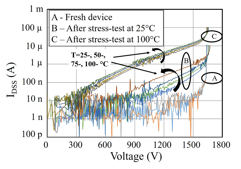
Fig. 2. LDSS measurements taken at 25° C, 50° C, 75° C, and 100° C for fresh devices, as well as degraded devices after stress tests conducted at ambient temperatures of 25° C and 100° C. The degraded devices show a further leakage increase at elevated temperatures.
